The advent of the integrated circuit (IC) in 1958 marked a paradigm shift in semiconductor fabrication, spurring technological advancements in microchip manufacturing. Ever since, the demand for miniaturization coupled with enhanced power fostered innovations in lithography, doping, and packaging. In 1965, the co-founder of Intel, Gordon Moore, coined the concept of Moore’s Law.
The rule states that the number of transistors on a chip doubles approximately every two years, while the cost per transistor drops. This has led to integration of higher component densities in ICs through advancements such as FinFET transistors, multi-gate structures, and 3D stacking technologies to create increasingly efficient, powerful, and portable devices that dominate modern life.
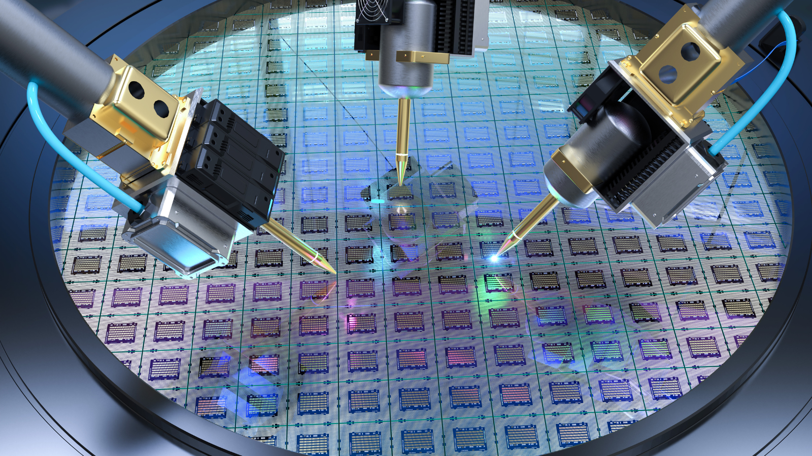
A Brief History of Microchip Fabrication
By the 1970s, MOSFETs (metal-oxide-semiconductor field-effect transistors) were developed and commercialized, leading to the next catalyst for the miniaturization of electronic devices. Traditionally, a thin layer of silicon dioxide (SiO2) is employed as an interlayer dielectric (ILD) via chemical vapor deposition (CVD) or other techniques to act as an insulator, typically deposited directly atop the MOSFETs and other chip constituents.
Despite silicon oxide’s exceptional insulating capabilities, it has serious limitations as a gate dielectric for today’s miniature, ultra-high performance devices. In particular, as transistor dimensions diminish, the layers of silicon oxide must follow suit, making them less effective. Specifically, thinner silicon oxide layers lead to increased current leakage, which slows circuit operation, limits voltage levels, lowers mobility, and hinders reliability.
Understanding Silicon Oxide and Its Limitations
Silicon is the primary material used in the chip fabrication process. This is due to its natural abundance, relatively low cost and safe manipulation. When silicon oxide is used independently in modern gate dielectrics, it has several limitations, including:
- Current leakage
- Difficulty in scaling
- Low capacitance control
- High chance of voltage breakdowns
To fully comprehend the limitations of silicon oxide in chip manufacturing, it’s important to understand the chip fabrication process:
- A CAD design of the circuit’s layout is created, including how the interconnects, transistors, and other components should be.
- The design is transferred onto a silicon wafer using photolithography, a photoresist and circuit pattern are applied, and UV light is used to etch the pattern into the photoresist.
- Unwanted material is removed via chemical or plasma etching.
- Doping alters the silicon’s electrical properties to form the transistor’s channel, drain, and source regions.
- Thin layers are deposited onto the silicon wafer as protective coatings, insulating layers, or conductive interconnects. Even when high-k dielectrics are employed, engineers use a thin layer of silicon oxide as a spacer material or interface between the high-k dielectric and the silicon substrate.
- Additional layers of high-k dielectrics are added as necessary using photolithography.
- Metal interconnects, usually fashioned from copper or aluminum, are deposited, patterned, and etched into different chip components to enable electric currents to flow between them.
- Testing takes place and defective chips are separated from good chips.
- An extra layer of quality control verifies that chips work optimally.
Cleaning happens at several stages of the fabrication process, and diffusion and planarization are also important steps. As microchips shrink, the need for stricter cleaning protocols and quality control measures drastically increases as defects and contaminants that were once insignificant must now be accounted for.
Other challenges caused by shrinking chip sizes include:
- Increased power leakage
- More variability in transistor characteristics
- Reduced carrier mobility
- Inefficient heat dissipation
- Increased crosstalk and resistance
- Higher costs due to increased complexity
How High-K Dielectrics Benefit Microchip Construction
High-k materials have been used for the past 15 to 20 years and boast numerous advantages as gate dielectrics in MOSFETs. Below are some benefits of applying a high-k dielectric layer directly over the silicon oxide layer:
- Acts as a powerful insulating material that reduces effective oxide thickness (EOT), preventing electrical current leakage and reducing power consumption.
- Whereas silicon dioxide has a dielectric constant of approximately 4, high-k dielectrics like lanthanum oxide have dielectric constants of around 20-30, meaning the finished chip can store significantly more charge.
- Chipmakers can scale transistor dimensions without impacting performance.
- The high dielectric constant means improved electrostatic control of the transistor gate, enhancing switching speed and boosting performance.
- High-k dielectrics are less susceptible to degradation and have improved resistance to hot carrier injection, which enhances a chip's reliability and lifespan.
Other uses of high-k dielectrics in chipmaking include:
- Gate dielectrics
- Ferroelectric memories
- Integrated passive devices
- Capacitors
- Microelectromechanical systems
- Interconnect insulation
The relatively low dielectric constant (k) of silicon dioxide (SiO2) makes it inadequate to sustain the required capacitance as semiconductor devices undergo further miniaturization. High-k dielectrics, characterized by their high permittivity, have emerged as pivotal in bolstering integration density, limiting power dissipation, and increasing performance attributes concomitant with the diminution in feature sizes. High-k materials, such as Hafnium Oxide (HfO2), are instrumental in mitigating gate leakage currents due to their superior ability to sustain stronger electric field coupling across the gate oxide. The integration of high-k dielectrics into MOSFET gate stacks is vital for the ongoing evolution of microchips that are increasingly compact, sophisticated, and energy-efficient.
The Role of Lanthanum Oxide in Microchips
Lanthanum-containing precursors show particular promise for improving microchips' dielectric performance. Lanthanum oxide has a relatively high dielectric constant of 27, and there are multiple lanthanum-containing precursors available, making it an attractive choice for manufacturers. Deposition techniques used to prepare these high-powered dielectric layers include:
- Chemical vapor deposition (CVD)
- Plasma-enhanced chemical vapor deposition (PECVD)
- Atomic layer deposition (ALD)
Of the three techniques, ALD has been used most successfully. This meticulously precise deposition method enables layer-by-layer growth of ultra-fine films that display atomic-level control.
Researchers have successfully used lanthanum-based ALD precursors in combination with water to create lanthanum oxide dielectric films with very low leakage currents of less than 10-8 A/cm2 at a frequency of 2 Mv/cm and a dielectric breakdown of 4.2 Mv/cm. The dielectric breakdown is the maximum electric field strength a high-k material can withstand before it breaks down and renders the material conductive.
Lanthanum precursors have also been used in combination with water and trimethylaluminum to afford a mixed dielectric layer of LaxAl2-xOy, which has even lower leakage currents at similar dielectric breakdown levels. Lanthanum makes an excellent ALD precursor because it's thermally stable, compatible with silicon, water reactive, and has sufficient volatility.
The Evolution of High-K Dielectric Deposition Precursors
As microchips have shrunk, the layers of silicon oxide that form electric barriers between components have become too thin to prevent leakage and maintain performance and efficiency. By applying a thin insulating layer of a high-k dielectric material such as lanthanum oxide on top of the silicon oxide, the EOT can be reduced while the desired capacitance is maintained. Ascensus is proud to provide partners access to lanthanum oxide. Reach out to our team to request a bulk quote today.